PCBA is the process of manual soldering electronic component onto a printed circuit boards (PCB) to create an electronic device. PCBA is a key part of electronic manufacturing services, which involve the assembly of electronic components onto printed circuit boards (PCBs) to create functional electronic devices. The PCB assembly services involves attaching components to the circuit board, which is usually made of a non-conductive substrate material with copper tracks that form the electrical connections. This process starts with a bare board before any components are mounted. Once the components are soldered, the PCB is typically coated with a layer of solder mask, which helps to protect the exposed copper layer from corrosion and gives the board its characteristic green color.
The PCBA manufacturing process can involve various techniques, such as surface mount technology (SMT) for surface mount components, and through-hole assembly for thru hole components. SMT assembly uses a pick and place machine to position components onto the PCB surface, followed by reflow soldering to secure them in place. Through-hole assembly involves inserting component pins through holes in the board and soldering them on the opposite side.
Although PCBA is most commonly associated with manufacturing electronics, it can also be used to create electrical components such as motors and transformers. In recent years, technological advances have led to the development of new methods for fabricating circuit board, making PCB assembly process more affordable and accessible than ever before. As a result, this versatile manufacturing technique is now used in various industries, from aerospace to medical devices.
What Is the Difference Between PCB and PCBA?
While often used interchangeably, PCB and PCBA refer to different stages in the electronics manufacturing lifecycle. A PCB board is a blank circuit board with no components attached—essentially the skeleton of any electronic device. Once electronic components are mounted onto the PCB surface, the result becomes a PCBA board or printed circuit board assembly.
This distinction is important in the electronics industry, especially during procurement and design phases. A printed circuit board alone is not functional. It’s only after mounting electronic components—through surface mount technology (SMT) or through-hole insertion—that it transforms into a complete circuit board.
The Different Types of Printed Circuit Boards Assembly (PCBA)
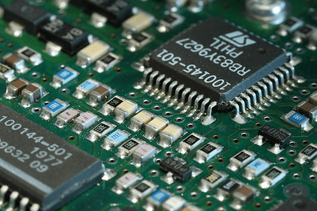
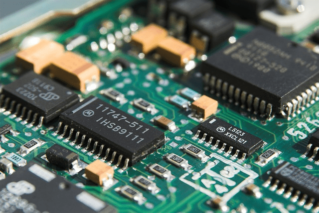
The acronym PCB stands for Printed Circuit Boards. A PCBA is a PCB that has undergone the process of having electronic component soldered onto it. This involves mounting all the necessary electronic components to form a complete and functional circuit. Unlike a finished electronic device, a PCBA may not have a housing or be able to function on its own, but it forms the basis of any electronic device imaginable. Many companies opt for contract manufacturing to handle their PCBA needs, leveraging the expertise and resources of specialized service providers.
There are two main types of PCBAs: through-hole and surface-mount. Through-hole PCBAs have holes drilled through the board for component leads to be inserted and soldered on the opposite side. Surface-mount PCBAs, on the other hand, have pads on the surface of the board where components are directly soldered using smt assembly techniques. The type of components used will determine the type of PCBA required and the size/density of the design.
Through-hole PCBAs are generally less expensive and easier to work with than surface-mount PCBAs, but they’re not as commonly used in today’s electronics because they tend to be larger and less dense than surface-mount boards. As a result, surface-mount technology (SMT) has largely replaced through-hole technology in recent years, and most new electronic designs use surface mount components and PCBAs.
Mixed assembly, which combines both surface mount and through hole components on the same board, is also used in some cases to achieve the best balance of cost, performance, and manufacturability.
How Surface Mount Technology Revolutionized PCB Assembly
Surface mount technology (SMT) has revolutionized PCB assembly by enabling the direct placement of electronic components on the PCB surface, eliminating the need for drilling holes. SMT supports higher component density, enabling miniaturization of devices and faster automated assembly.
SMT is the preferred method for assembling consumer electronics, wearable tech, and medical instruments. Companies like Vergent Products utilize advanced SMT lines to handle fine-pitch and BGA components with high precision, improving overall production efficiency and product quality.
How Printed Circuit Boards (PCBs) Are Used in Electronic Components?
Printed circuit boards (PCBs) support and connect electronic component using conductive tracks, pads, and features etched from copper layers laminated onto a insulators material. PCBA is a crucial part of electronic assembly, where various components are mounted onto a PCB to create a complete electronic circuit, which may involve multiple layers of dielectric material and conductive traces.
The PCB assembly process results in a board with embedded capacitors, resistors, and other active and passive components, forming a complete electronic circuit. PCBA is used in a wide range of electrical devices such as mobile phones, TVs, laptops, as well as medical devices like pacemakers and defibrillators.
PCBA offers many advantages over other electronic packaging methods, including improved reliability, smaller size, lighter weight, and higher performance. It is also easier to repair and replace individual components on a PCBA compared to other types of electronic packaging.
The use of automated assembly processes, such as pick and place machines, reflow soldering, and wave soldering, allows for the production of PCBAs with consistent quality and efficiency. Automatic optical inspection (AOI) systems are often used to detect any misplaced components, solder blobs, or other defects that could affect the proper functionality of the board that has been assembled.
How Does PCB Fabrication Fit Into the Assembly Process?
PCB fabrication is the precursor to the pcb assembly process, involving the creation of printed circuits, conductive layers, and insulating material that form the base of the board. This process typically includes the lamination of copper onto a substrate, etching of traces, drilling of holes, and applying a solder mask.
Only after the fabrication phase is complete can assembly methods begin—either for flexible PCBs, two layer boards, or more advanced multi layer PCBs. Fabrication defines the board’s layout, while assembly adds functionality by placing the necessary electronic components and forming solder joints.
The process of PCB assembly
Printed wiring board assembly, or PCBA, is the process of soldering electronic components to a PCB to ensure proper electrical connectivity and physical support. Many PCBA providers offer turnkey solutions, handling everything from component sourcing to final assembly and testing. The first step in the PCB assembly process is to print a thin layer of solder paste onto the board using a solder paste printer. The solder paste printing contains tiny beads of solder that will later melt to form the electrical connections.
Next, the components are placed onto the board using a pick and place machine, which accurately positions each component based on the design file. The board then goes through a reflow oven, which melts the solder paste and permanently attaches the components to the PCB.
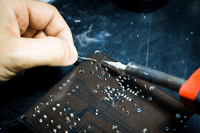
After reflow soldering, the assembled board may undergo additional processes such as wave soldering for through hole components, manual soldering for special or large parts, and conformal coating for added protection.
Throughout the PCBA process, various inspections and tests are performed to ensure the quality and functionality of the final product. Solder paste inspection (SPI) checks the accuracy of the solder paste printing, while automated optical inspection (AOI) verifies the correct component placement and orientation of components.
In-circuit testing (ICT) and functional testing may also be performed to verify the electrical properties and performance of the assembled board. The entire process of PCBA is critical for ensuring that electronic devices function correctly and reliably. Proper soldering and assembly techniques help to prevent issues such as solder blobs, cold solder joints, and component failures that could lead to device malfunctions or safety hazards.
Why Component Placement Matters in PCB Assembly
Component placement is a critical step in the assembly process and directly affects signal integrity, heat dissipation, and manufacturability. Proper inserting component leads and positioning of surface mount devices ensure that electronic components mounted on the board perform reliably.
High-speed designs especially benefit from precise placement, as even a slight misalignment can result in signal timing issues. Advanced tools like automated optical inspection (AOI) systems check the printed circuit assembly to verify correct alignment and orientation of all components.
What Role Does Functional Testing Play in PCBA Quality?
Functional testing ensures that the complete circuit board operates as intended. This stage verifies not only the presence of all functional components, but also that each element correctly communicates with others to electrically connect electronic components across the board.
Combined with in-circuit testing and AOI, functional tests are essential for identifying errors in complex pcb and pcba systems. Whether it’s checking voltage thresholds, signal outputs, or operational behaviors, functional testing validates the entire assembly process.
What Are the Most Common Assembly Methods in PCBA?
Common assembly methods include:
- Surface Mount Technology (SMT)
- Through-Hole Technology (THT)
- Mixed Technology Assembly
- BGA Assembly
- Manual Soldering for complex parts
Each method serves different design goals. For example, SMT is ideal for high-speed, compact electronics, while THT provides stronger mechanical bonds for connectors and large components.
Vergent Products supports all these methods and employs state-of-the-art soldering chemistries including No-Clean, Water Soluble, and Leaded/RoHS-compliant processes.
Advantages and Disadvantages of PCBA
Printed Circuit Boards (PCBs) are thin plates that support and electrically connect electronic components using conductive pathways, typically made of Copper tracks. They are found in nearly all types of electronic equipment, from calculators and computers to televisions and cell phones.
One of the main advantages of using PCBs over other types of electronic packaging is their small size and lightweight nature, which allows for more compact and portable devices. Additionally, the use of automated assembly processes enables the production of PCBs at a low cost per unit.
PCBs also offer improved reliability and consistency compared to other assembly methods, as the standardized manufacturing process minimizes the risk of human error and ensures uniform quality across multiple boards. Implementing design for manufacturability principles can help mitigate these issues by optimizing the PCB layout for efficient and reliable production.
However, there are also some disadvantages to using PCBs. The conductive traces on a PCB can be easily damaged by impact, heat, or moisture, making repairs difficult and costly. If the component layout on a PCB is not carefully designed, it can lead to signal interference, crosstalk, and other issues that may affect the performance and reliability of the device.
Another potential disadvantage is the initial setup cost for PCB assembly process, which can be higher than other methods due to the need for specialized equipment and skilled labor. This can make PCBAs less cost-effective for low-volume production runs or prototype designs.
Despite these drawbacks, the benefits of PCBAs in terms of size, weight, reliability, and manufacturability make them the preferred choice for most electronic devices today. As technology continues to advance, new materials and techniques are being developed to address some of the limitations of traditional PCBs, such as the use of flexible or rigid-flex substrates for improved durability and design flexibility.
Why PCB and PCBA Matter in Modern Electronics
From flexible PCBs in wearable tech to multi layer PCBs in aerospace systems, both PCB and PCBA are essential to the electronics industry. These components serve as the backbone for everything from consumer electronics to industrial control systems.
A printed circuit board without mounted parts is merely a framework, while the pcba board includes electronic components attached and tested to perform specific functions. Their synergy supports rapid innovation in technology and drives down cost through scalable pcb assembly services.
Who should use PCBA services?
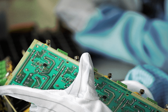
Printed circuit board assembly (PCBA) is a critical process in the manufacturing of electronic devices, as it involves soldering components onto a printed circuit board to create a functional electronic assembly. While some companies have in-house PCBA capabilities, many others choose to outsource this process to specialized PCBA service providers.
PCBA services are ideal for companies that lack the necessary equipment, expertise, or capacity to handle PCB assembly in-house. This includes startups, small businesses, and even larger companies that prefer to focus on their core competencies while leaving the manufacturing to experts. Outsourcing PCBA is particularly beneficial for prototype development, allowing companies to quickly and cost-effectively test new designs.
Outsourcing PCBA can provide many benefits, such as access to advanced technology, improved quality control, faster turnaround times, and cost savings through economies of scale. PCBA service providers often have a wide range of capabilities, including mount surface assembly, through-hole assembly, mixed technology assembly, and more.
When selecting a PCBA service provider, it is essential to consider factors such as experience, quality control processes, certifications, and customer support. Look for a provider that has a proven track record of success in your industry, and that can offer the specific services and expertise that your project requires.
Vergent Products’ Expert PCBA Services
![]()
Vergent Products is your go-to PCB manufacturers. We have a team of highly skilled engineers and technicians who specialize in printed circuit board assembly. We offer a full range of PCBA services, from design and prototyping to full-scale production and testing. Our state-of-the-art equipment and rigorous quality assurance processes ensure that every board we assemble meets the highest standards of reliability and performance.
In addition to PCBA, we also offer box build assembly services, providing a complete solution from component assembly to final product integration.
Whether you are a startup looking to bring a new product to market, or an established company in need of high-volume PCBA, we have the expertise and resources to meet your needs. Contact us today to learn more about how we can help turn your electronic designs into reality.